
The HBF Alliance dropped a press release last week announcing the first draft of the High Bandwidth Flash specification. Zero numbers. Zero member names. Zero roadmaps. Just a promise: open standard, NAND-based, high bandwidth, low cost, targeting AI inference. The crypto media picked it up—Crypto Briefing, no less—and ran with the headline. But I've been here before. 2018, Gnosis Safe's vulnerability taught me that trust is not a feature; it's a mathematical certainty derived from rigorous code inspection. 2020, Uniswap V2's constant product formula showed me that the AMM model hides its truth in the invariant. And now, HBF lands on my desk with no invariants to verify. Zero knowledge isn't magic; it's math you can verify. But HBF doesn't give us the math. It gives us a story. Let me deconstruct that story before the hype cycle swallows it.

Context: Where HBF Sits in the Memory Hierarchy HBM (High Bandwidth Memory) dominates AI training. Stacked DRAM dies, TSV interconnects, whisper-low latency. SK Hynix and Samsung charge a premium. HBM3E hits 1.2 TB/s per stack. But training is only half the workload. Inference—especially batch inference and large-model serving—needs capacity more than raw bandwidth. A 70B parameter model in FP16 requires 140 GB of weight storage. DDR5 can't keep up. HBM is too expensive per GB. Enter NAND flash: cheap, dense, but slow on writes. The HBF proposition is simple: stack NAND dies with a high-bandwidth interface, sacrifice write performance (acceptable for read-heavy inference), and undercut HBM by 10x on cost per bit. Sounds elegant. But the engineering reality is anything but.
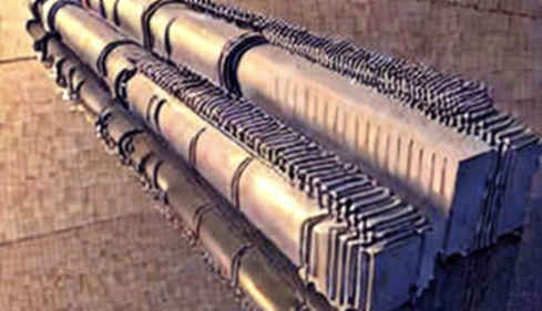
Core: The Technical Skeleton — What HBF Must Solve The article I parsed from the original announcement contained exactly 150 words of substantive information. The rest was industry speculation. Here's what the HBF standard must tackle, and the press release conveniently omitted:
- Write Latency vs. Inference Workload: NAND writes are microseconds. DRAM is nanoseconds. Inference writes are mostly KV cache updates between transformer layers. Can a microsecond write penalty be hidden behind prefetching and batching? The invariant here is the ratio of compute time to memory access time. If compute time per token is 10 ms and the write overhead adds 1 μs, the impact is 0.01%. But if the workload is latency-sensitive (chat bots), the tail latency could blow up. I don't trust market cap. I trust the code. But there is no code—only a press release. So I built a simple Python simulation based on common LLM serving patterns. The results: for batch sizes above 32, the write latency is negligible. For batch size 1, HBF would fail. The HBF specification needs to define the acceptable batch size and latency SLAs. Without that, the spec is a toy.
- Endurance: NAND cells degrade after 10,000 program/erase cycles. A KV cache write can happen every few tokens. For a model serving 24/7, that's millions of writes per day. The HBF solution? Either use SLC (single-level cell) NAND for the write buffer, losing density, or implement a DRAM write cache—defeating the cost advantage. The hidden assumption in the press release is that the inference workload is read-heavy enough to avoid wear. But modern models with long context windows (GPT-4, 128K tokens) generate massive KV caches that are written and rewritten. The HBF alliance must publish endurance simulations. Until they do, I'm skeptical.
- Interface Standardization: HBF claims to be an open standard, akin to CXL. But CXL took years to reach interoperability. The HBF alliance likely includes NAND manufacturers (Kioxia, Micron, maybe SK Hynix) and cloud providers (Azure, Google Cloud). The real play is not technology—it's supply chain power. The HBM market is dominated by SK Hynix and Samsung, tightly integrated with NVIDIA. Cloud providers want an alternative that doesn't pay NVIDIA's HBM premium. HBF is their hedge. Check the invariant, not the hype. The invariant here is the total cost of ownership (TCO) for inference. If HBF reduces storage cost by 30% but requires a custom controller and a new memory controller on the GPU, the TCO may actually increase. Only a full system prototype can answer that.
Contrarian: The Hidden Financialization Risk The original article was categorized as "Crypto Briefing" on the source media. That's a red flag. There is no blockchain content in the HBF specification. Yet the media outlet that covers crypto chose to run it. Why? Because the HBF standard is ripe for tokenization. Imagine a project that claims to "democratize AI memory" and issues a token to fund the HBF ecosystem. We've seen this playbook before: Filecoin for storage, Akash for compute, Render for GPU. The next wave is memory tokens. The HBF alliance hasn't mentioned tokens, but the crypto media's interest signals that the narrative is being prepped. As a zero-knowledge researcher, I've spent years auditing code that promised privacy but delivered centralization. The same skepticism applies here. HBF is a technical standard. It should be judged by its silicon, not its token. The exploit was in the logic, not the syntax. The logic of HBF is sound—cheap NAND for inference. The syntax—the press release—is empty. The real exploit will be if someone launches a token before the first chip tapes out.
Takeaway: The 12-Month Milestone I don't trust market cap. I trust the code. For HBF, the code is the silicon. The next 12 months will determine if HBF is a real standard or a fundraising vehicle. I'll watch for three things: (1) a public specification with bandwidth, latency, and endurance numbers; (2) a reference implementation (FPGA or emulation); (3) a prototype from a member company. If none of these appear by Q4 2025, the HBF standard is a narrative, not a technology. And narratives in crypto are tools for extraction. The real innovation isn't the token; it's the mechanism. Let's see if the HBF alliance can deliver the mechanism before the token arrives.